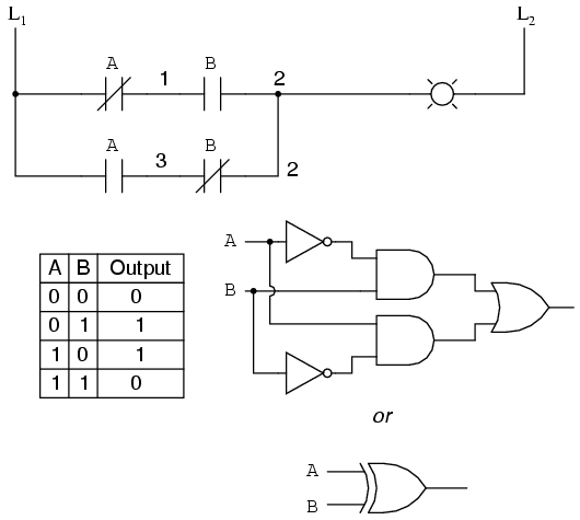
We can construct simply logic functions for our hypothetical lamp circuit, using multiple contacts, and document these circuits quite easily and understandably with additional rungs to our original “ladder.” If we use standard binary notation for the status of the switches and lamp (0 for unactuated or de-energized; 1 for actuated or energized), a truth table can be made to show how the logic works:
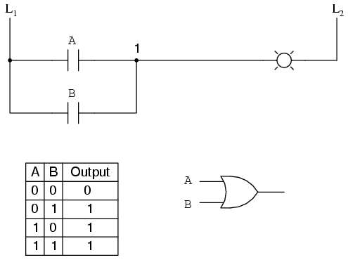
Now, the lamp will come on if either contact A or contact B is actuated, because all it takes for the lamp to be energized is to have at least one path for current from wire L1 to wire 1. What we have is a simple OR logic function, implemented with nothing more than contacts and a lamp.
We can mimic the AND logic function by wiring the two contacts in series instead of parallel:

Now, the lamp energizes only if contact A and contact B are simultaneously actuated. A path exists for current from wire L1 to the lamp (wire 2) if and only if both switch contacts are closed.
The logical inversion, or NOT, function can be performed on a contact input simply by using a normally-closed contact instead of a normally-open contact:
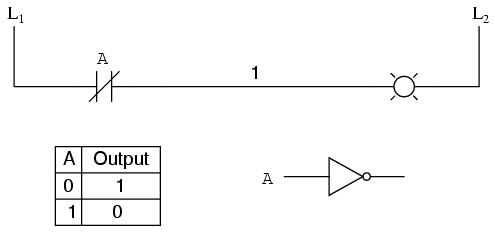
Now, the lamp energizes if the contact is not actuated, and de-energizes when the contact is actuated.
If we take our OR function and invert each “input” through the use of normally-closed contacts, we will end up with a NAND function. In a special branch of mathematics known as Boolean algebra, this effect of gate function identity changing with the inversion of input signals is described by DeMorgan’s Theorem, a subject to be explored in more detail in a later chapter.
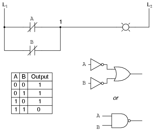
The lamp will be energized if either contact is unactuated. It will go out only if both contacts are actuated simultaneously.
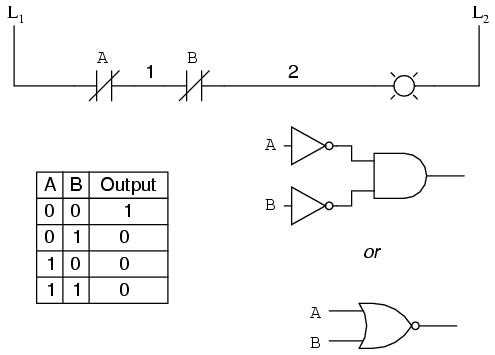
Likewise, if we take our AND function and invert each “input” through the use of normally-closed contacts, we will end up with a NOR function:
A pattern quickly reveals itself when ladder circuits are compared with their logic gate counterparts:
- Parallel contacts are equivalent to an OR gate.
- Series contacts are equivalent to an AND gate.
- Normally-closed contacts are equivalent to a NOT gate (inverter).
The top rung (NC contact A in series with NO contact B) is the equivalent of the top NOT/AND gate combination. The bottom rung (NO contact A in series with NC contact B) is the equivalent of the bottom NOT/AND gate combination. The parallel connection between the two rungs at wire number 2 forms the equivalent of the OR gate, in allowing either rung 1 or rung 2 to energize the lamp.
To make the Exclusive-OR function, we had to use two contacts per input: one for direct input and the other for “inverted” input. The two “A” contacts are physically actuated by the same mechanism, as are the two “B” contacts. The common association between contacts is denoted by the label of the contact. There is no limit to how many contacts per switch can be represented in a ladder diagram, as each new contact on any switch or relay (either normally-open or normally-closed) used in the diagram is simply marked with the same label.
Sometimes, multiple contacts on a single switch (or relay) are designated by a compound labels, such as “A-1” and “A-2” instead of two “A” labels. This may be especially useful if you want to specifically designate which set of contacts on each switch or relay is being used for which part of a circuit. For simplicity’s sake, I’ll refrain from such elaborate labeling in this lesson. If you see a common label for multiple contacts, you know those contacts are all actuated by the same mechanism.
If we wish to invert the output of any switch-generated logic function, we must use a relay with a normally-closed contact. For instance, if we want to energize a load based on the inverse, or NOT, of a normally-open contact, we could do this:
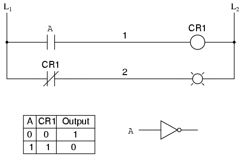
We will call the relay, “control relay 1,” or CR1. When the coil of CR1 (symbolized with the pair of parentheses on the first rung) is energized, the contact on the second rung opens, thus de-energizing the lamp. From switch A to the coil of CR1, the logic function is noninverted. The normally-closed contact actuated by relay coil CR1 provides a logical inverter function to drive the lamp opposite that of the switch’s actuation status.
Applying this inversion strategy to one of our inverted-input functions created earlier, such as the OR-to-NAND, we can invert the output with a relay to create a noninverted function:
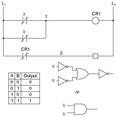
From the switches to the coil of CR1, the logical function is that of a NAND gate. CR1‘s normally-closed contact provides one final inversion to turn the NAND function into an AND function.
Comments
Post a Comment